1. The definition of processing levels is not clear.
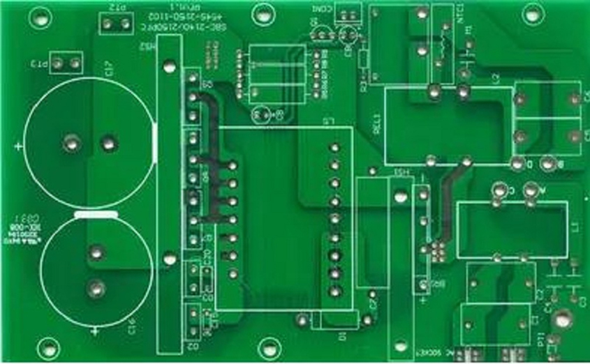
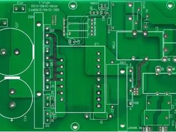
Design a single panel on the TOP layer, and if there is no explanation for the front and back design, the resulting board may not be easily soldered onto the equipment.
2. The large area of copper foil is too close to the outer frame.
A distance of at least 0.2 millimeters should be ensured between the large area copper foil and the outer frame, as milling onto the copper foil during shape milling can easily lead to copper foil warping and solder resist detachment.
3. Draw solder pads with filler blocks.
When using filler blocks to draw solder pads, DRC can be used for inspection during circuit design, but it is not feasible for processing. Therefore, this type of solder pad cannot directly generate solder mask data. When applying solder mask, the filler block area will be covered by solder mask, causing difficulty in device welding.
4. The electrical layer is both a solder pad and a connecting wire.
Due to the design of a flower pad power supply, the ground layer is opposite to the image on the actual printed board, and all connections are isolation lines. When drawing several sets of power supplies or ground isolation lines, be careful not to leave any gaps, causing a short circuit between the two sets of power supplies, and the connection area cannot be blocked.
